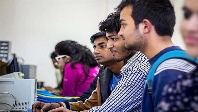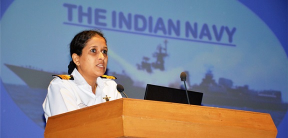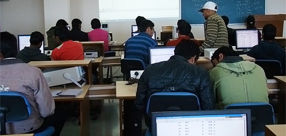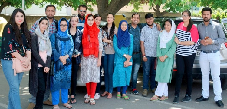
SMVDU Katra, May 2019. School of Electronics & Communication Engineering, Shri Mata Vaishno Devi University (SMVDU), Katra, organised an industrial visit to Semi-Conductor Laboratory, Chandigarh, Department of Space, Government of India for its M. Tech. Students to focus on design, development, fabrication, assembly & packaging, testing and quality assurance of CMOS and MEMS devices for satellite and other various applications. This industrial visit was coordinated by Dr. Sachin Kumar Gupta, Faculty, SoECE & Ms. Shaivya Manhas, Faculty, SoEM, along with Mr. B. K. Bhatia, T&P Officer, SMVDU. The visit started with the brief profile of SCL by Mr. Sanjay Bhatnagar, Engineer' SF'-PPMD at Semi-Conductor Laboratory. He presented a short video clip pertaining to major contributions, achievements, and campus life of SCL. Later, he discussed the design process for fabrication of ICs, Mixed Signal and Analog ASIC Design, and Wide spectrum industry standard EDA tools. The students were taken to various labs which includes 8" Wafer Fabrication Facility (Clean Rooms of Class 1, 10, 100 and 1000 with controlled environmental conditions), Assembly & Packaging (Fine Pitch Bonding capability for pad size of 57µmx57µm and 65µm pitch, Low Temperature Process for packaging large dies, Multi-Chip Packaging Process for ASICs and sensor devices, MIC Packaging), Reliability & Quality Assurance (Facility for Environmental Test, Facility for Failure Analysis), etc. The industrial tour was very informative, enriching, and imparted a great learning experience to the students.

 Mr. Yogesh Declares Qualified for the Award of Ph.D....
 Ms. Amina Khan awarded PhD in Electronics and Communication Engineering...
 Ms. Haneet Kour Declared Qualified for the Award of Ph.D...
 Mr. Shubham Mahajan Declares Qualified for the Award of Ph.D...
 Ms. Misbah Shafi Declares Qualified for the Award of the Ph.D...
 Dr Gupta of SMVDU Delivers a Talk at Banasthali Vidyapith..
 Mr Vikram Kumar, Research Student, Declares Qualified for the Ph.D...
 SMVDU Scholar Presents in International Conference on Innovations in Computing..
 Paper Publication by SMVDU Student and Faculty in SCI Journal..
 Ms. Shagun Gupta Declares Qualified for the Award of Ph.D...
